Custom artwork footprints on PCBs
Many people that design PCBs want to include artwork on their boards, whether as silkscreen or a footprint. Most CAD softwares include native support for processing arbitrary images into CAD objects that can be placed on different board layers. I’ll use KiCad for this tutorial, but the general steps are nearly analogous in other design platforms.
Start by choosing the image you want on your board, and download it as a png/jpg. Here’s the image we’ll be using:

Next, open up KiCad and go into the Image Converter tool. Click on Load Source Image, and open the image from your files. There are a few options you’ll see -
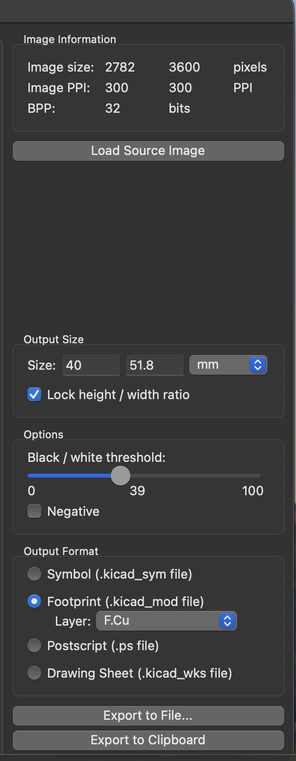
Generally, you want to keep the aspect ratio locked, unless you want the image to stretch in one direction. Change the size to your desired size (you can check this using the measure tool in your PCB). The easiest way to determine the black/white ratio is just to play around with it until the picture looks right. To create a footprint, save the output as a footprint on F.Cu (or B.Cu if you want it on the back of the board). Then click Export to File. Generally, it’s a good idea to keep a dedicated folder inside your KiCad directory for custom footprints, but it’s not required.
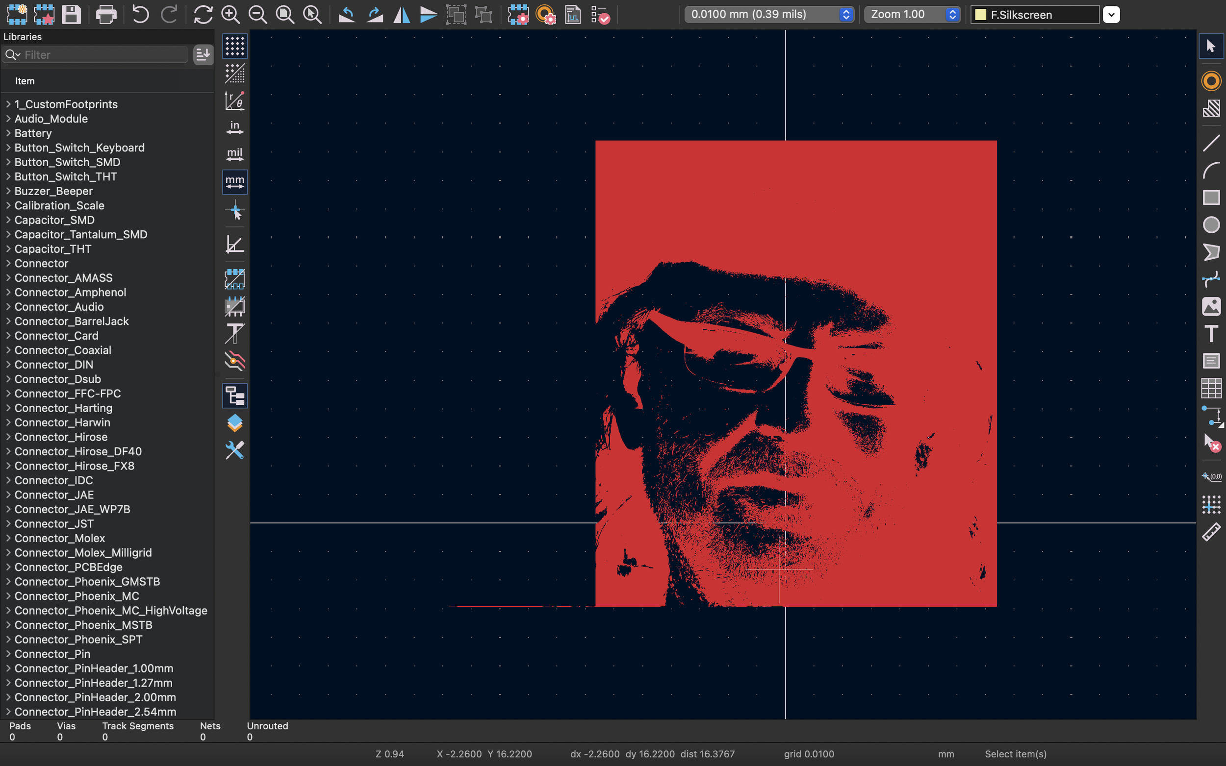
Next, you’ll open up the Footprint Editor tool in KiCad. Click File → Import → Footprint, and open the .kicad_mod file you just created. You’ll see something like this -
Now, hit save and save it to any footprint directory, preferably one dedicated for custom footprints. Now, you can go into the PCB editor. Place a footprint and choose your exported file from the footprint editor. Now, you’ll have your artwork on your board as a footprint!
Hey Baird
If you want the face to be exposed copper instead of copper with soldermask over it, make sure to add an F.Mask (or B.Mask if its on the back) layer in the footprint editor. To do so, you' can copy + paste your artwork shape in the same location, but change the layer to F.Mask/B.Mask. Since the mask layer is negative, adding the mask shape will result in the soldermask being removed in that shape. So, you’ll end up with exposed, finished copper rather than the copper with a thin layer of soldermask over it.
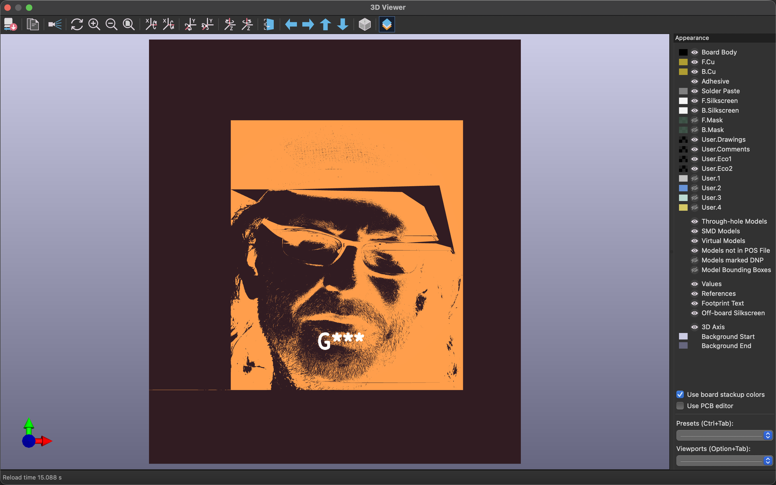
Complex images such as this can be a pain to work with, as KiCad often lags when trying to render them. But, if you can stick it out, you’ll have some nice, detailed images on your board!