Designing a custom PCB for this year’s Telethon
Last year’s Telethon was a great success, considering it was M5’s first annual event. I learned many things in the process regarding coordination, telephony, and analog electronics. However, I was still new to designing my own circuits, especially on a PCB. There were many things I wasn’t able to make in time for the Telethon, mainly a custom PCB that could sniff the phone lines and use that data for visualization and analysis purposes.
One year later, and I think I’m ready to take on the task this time.
Before I started any sort of PCB design, I needed to refresh my knowledge on Kicad. It’s been a while since I’ve last used Kicad, but this “Kicad 9.0 Getting Started” series by Digikey was an excellent refresher, I definitely recommend checking it out here: https://youtu.be/0WCi1rhueH4?list=PLEBQazB0HUyQ5YJSdCBb79orXaR3Uk5vm
After watching this series, I knew I needed to pick a good MCU to be the heart of the PCB. I initially wanted to settle on using the RP2350, but my colleague Ian suggested we look into an STM32 based MCU. I also agreed, mainly due to the RP2350 only supporting USB 1.1 by default, and we both wanted to utilize high speed USB to transfer data between this custom PCB and a Raspberry Pi that would handle the streaming/coordination. Luckily, I found a great resource for picking the right STM32 MCU, STM32CubeMX.
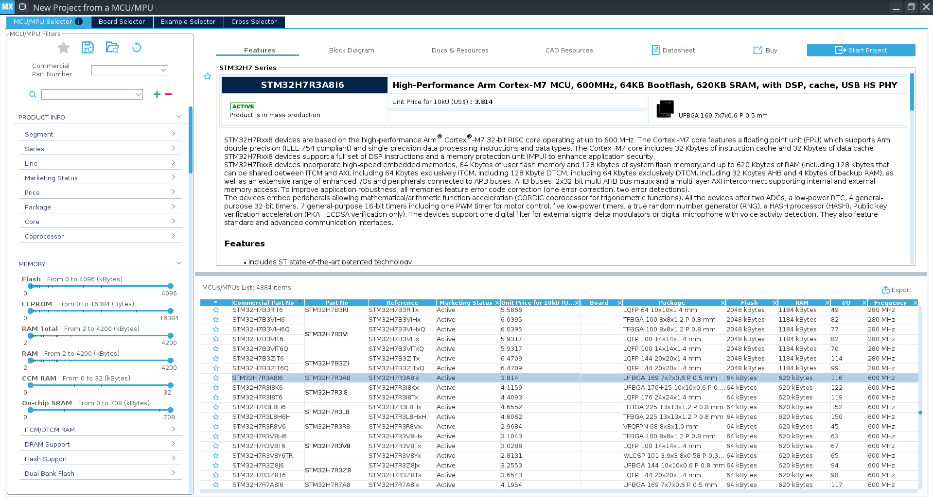
STM32CubeMX’s MCU Selector menu, which makes it super easy to find the right MCU for your project.
This made it super easy to find the right MCU. I wanted one with a high clock speed to handle multiple data streams (from the phones and to the Pi), enough SRAM to store multiple buffers of phone audio data, and built-in high speed USB to simplify our design. I settled on the STM32H7R3A8I6.
With the MCU picked, I got to work in Kicad:
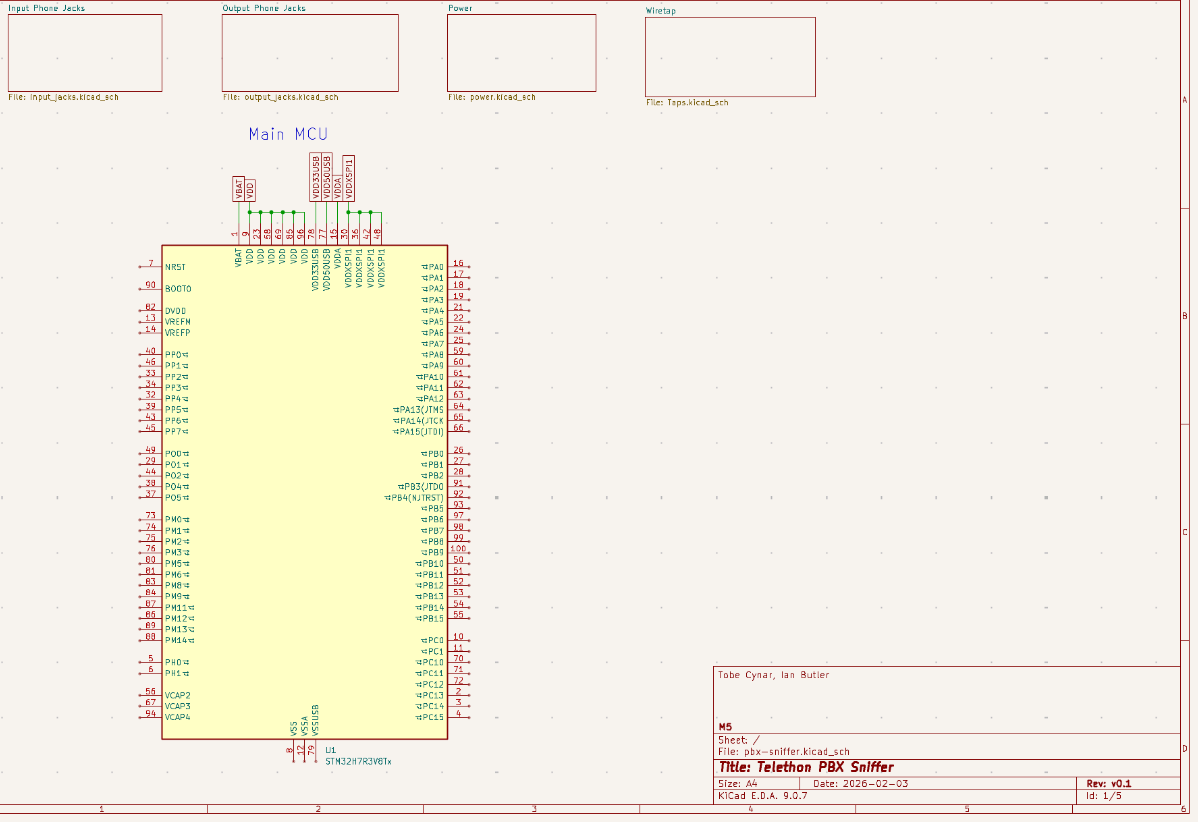
The main page of the schematic for the custom PCB.
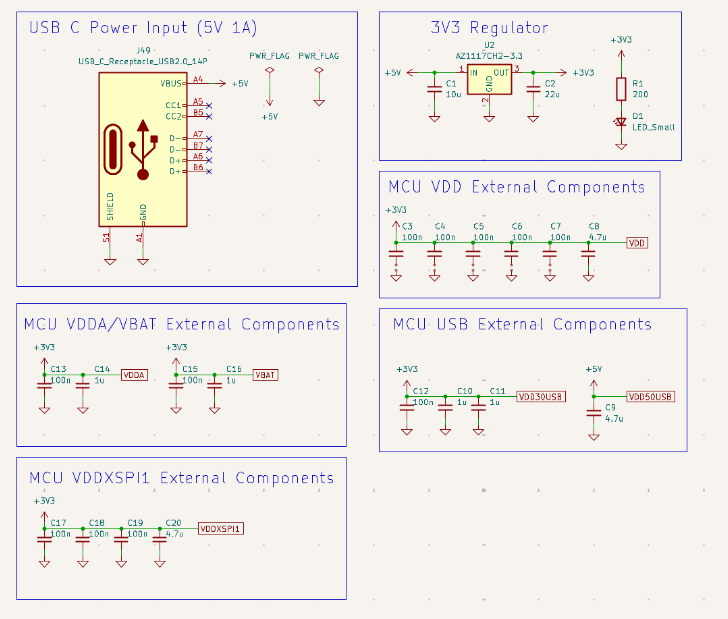
The external power components on a separate sheet in Kicad.
I quickly realized that all the circuitry for this PCB was not going to fit on a single page. I’ve never made a multi-sheet schematic before in Kicad, so I had to research the fundamentals of how it works, using Global Nets and Hierarchical Sheets to split up the schematic into many sheets. I also had to fit all 24 phone jacks onto a sheet, and figure out how to connect them all together!
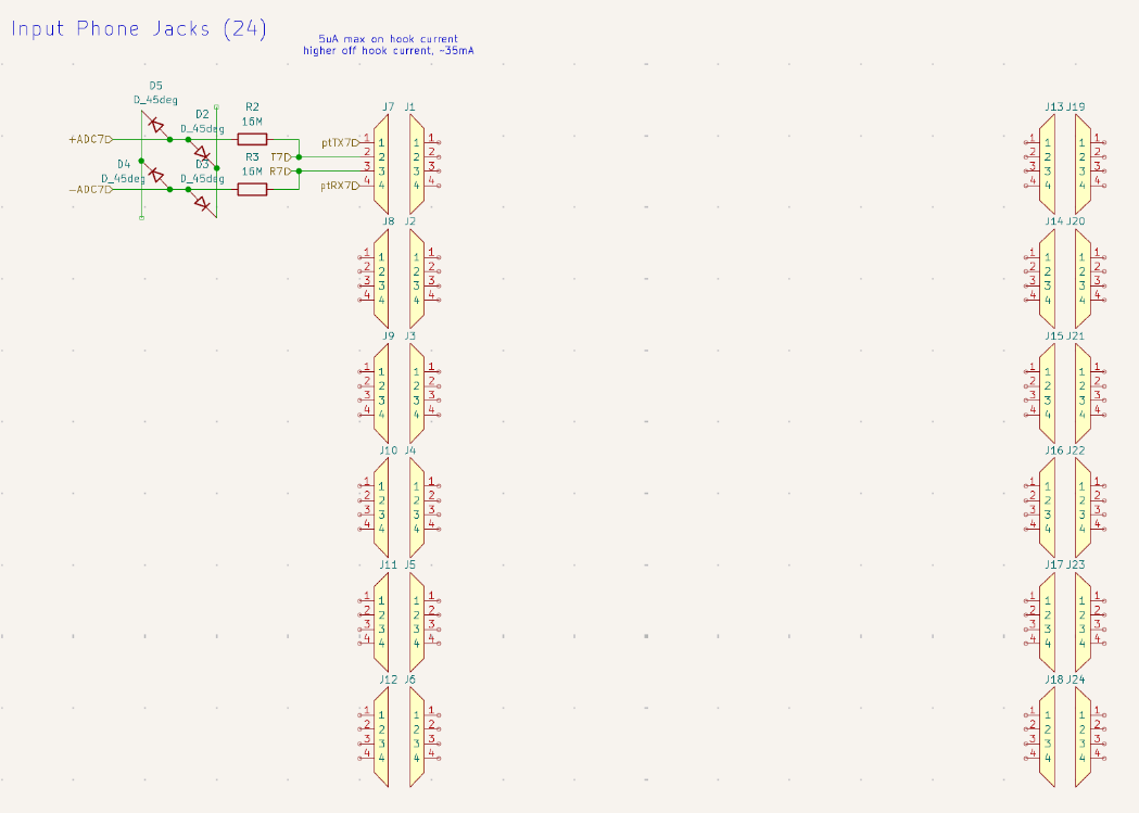
The input jacks for the phones, with an in-progress isolation schematic so the analog signals can be read without damaging the ADC.
I still have a lot to go… finishing the entire schematic, and somehow routing everything together in a neat way. Writing all the software for this device will also be a monumental task. I think I will be able to pull it off, especially with the help of Ian. If I can make this work, this will definitely be the most complicated thing I have ever designed and built.