Useful KiCad plugins: How we created the Telethon Sniffer PCB in under 24 hours
With the Telethon quickly approaching on April 25th, we had to seriously figure out how we were going to lay out our PCB with hundreds of components. We’ve been struggling for a couple weeks now to find an easy way to organize and tile the components in a way that would make routing as trivial as possible. It didn’t help that this was Ian and I’s first time at laying out a PCB of this size… On top of all this, on Thursday March 26th, we were told if it wasn’t done by Friday it wasn’t going to be ordered. Despite all odds, after an all-nighter and an all-dayer, we pulled it off… so how did we do it?
KiCad automation plugins seriously saved our butts!
Prior to Thursday, our PCB looked like this:
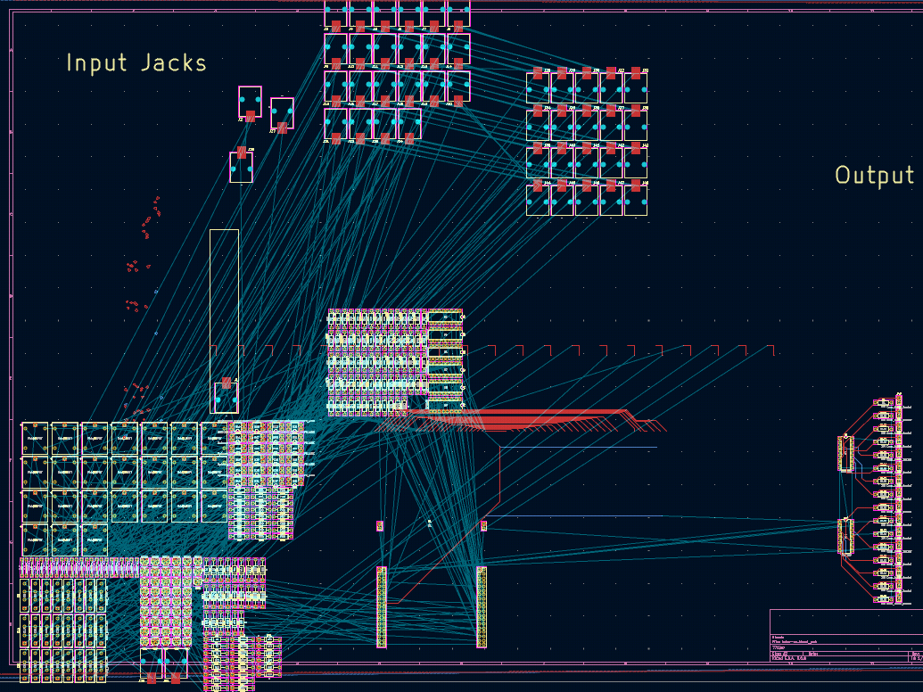
Our in progress PCB that we were having trouble even getting started on.
This isn’t exactly what it looked like, but it looked something like this, lots of grouped components sitting around, nothing really routed yet, etc. We were stuck on how we should continue from this point, considering KiCad didn’t really offer any tools to automate the placement of anything. So how did we go from that, to this?
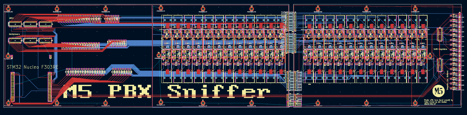
Our completed PCB design, which was made only 20ish hours later!
We used a few little-known plugins for KiCad that helped automate the placement of hierarchical components. They were as follows:
Place Footprints: Automate placing footprints in a linear, circular, or matrix arrangement
This one helped us place all the phone jacks, resistors, and other sequential components in a neat line with a spacing we could pick ourselves
Replicate Layout: Replicate layout of one hierarchical sheet to other copies of the same sheet
This was by far the most important one, since all the components for sniffing a single phone line was in its own hierarchical sheet, we could layout and route the components for one phone line, then replicate it to all 24 other phone lines! You can see the cascading phone jacks in the finished PCB above, all possible due to this plugin!
Fabrication Toolkit: Automate PCB fabrication process for JLCPCB
This one wasn’t strictly necessary, but it did automate changing settings and exporting gerber files for our PCB in a format that JLCPCB would prefer, which did save us some time
If you want to use these plugins for yourself, I you can find them from the first KiCad window you see when you open it (picture below), then Tools→Plugin and Content Manager.
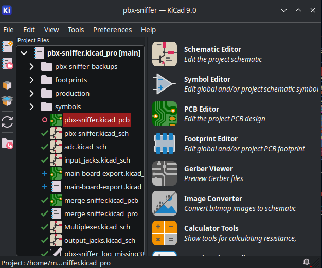
The first KiCad window you see when opening the program. Use the “Tools” tab at the top of the window.
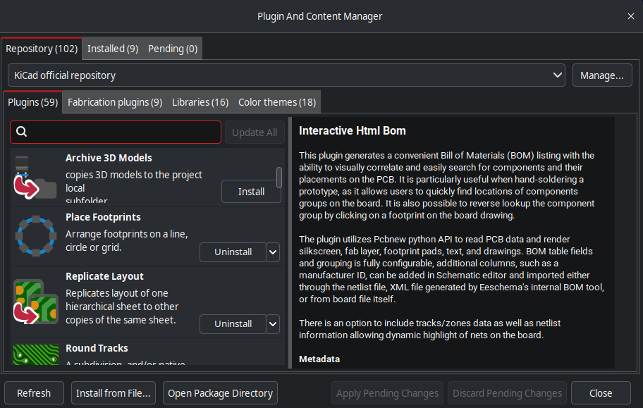
The Plugin and Content Manager window
There are plenty of other useful plugins here too, so be sure to check out everything offered here. For those interested, here is what the final PCB 3D render looks like:
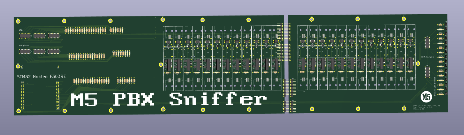
The 3D render of our board.
As you can see, we did have to split our board in half to fit within JLCPCB’s requirements, but that process was not as painful as I though it would be. When the board finally arrives, we will provide another update, but in the meantime we hope these plugins greatly improve your KiCad experience!