Beginning design of a VHF bandpass filter
Last semester, I built an antenna that would pick up an Automatic Picture Transmission (APT) signal from weather satellites operating in the ~140 MHz band. The pictures we got were pretty cool, but zooming in, you could see streaks of black pixels where the signal was lost or was not able to be decoded. The satellite uses Offset Quadrature Phase-Shift Keying (OQPSK) as a modulation technique, and being the digital scheme that is it, the signal will either be picked up perfectly or not at all. We have error correction to thank for that, but in either case, a filter and an amp on the frontend of the software-defined radio (SDR) wouldn’t be a bad idea in case I ever want to run the coax longer than a few feet.
Starting out with this design, I had to know what I wanted as a ‘wish list.’ Looking at the FCC spectrum allocation chart, there are some sources of potential noise pretty close to the slot at which the satellite operates - most notable, FM radio.
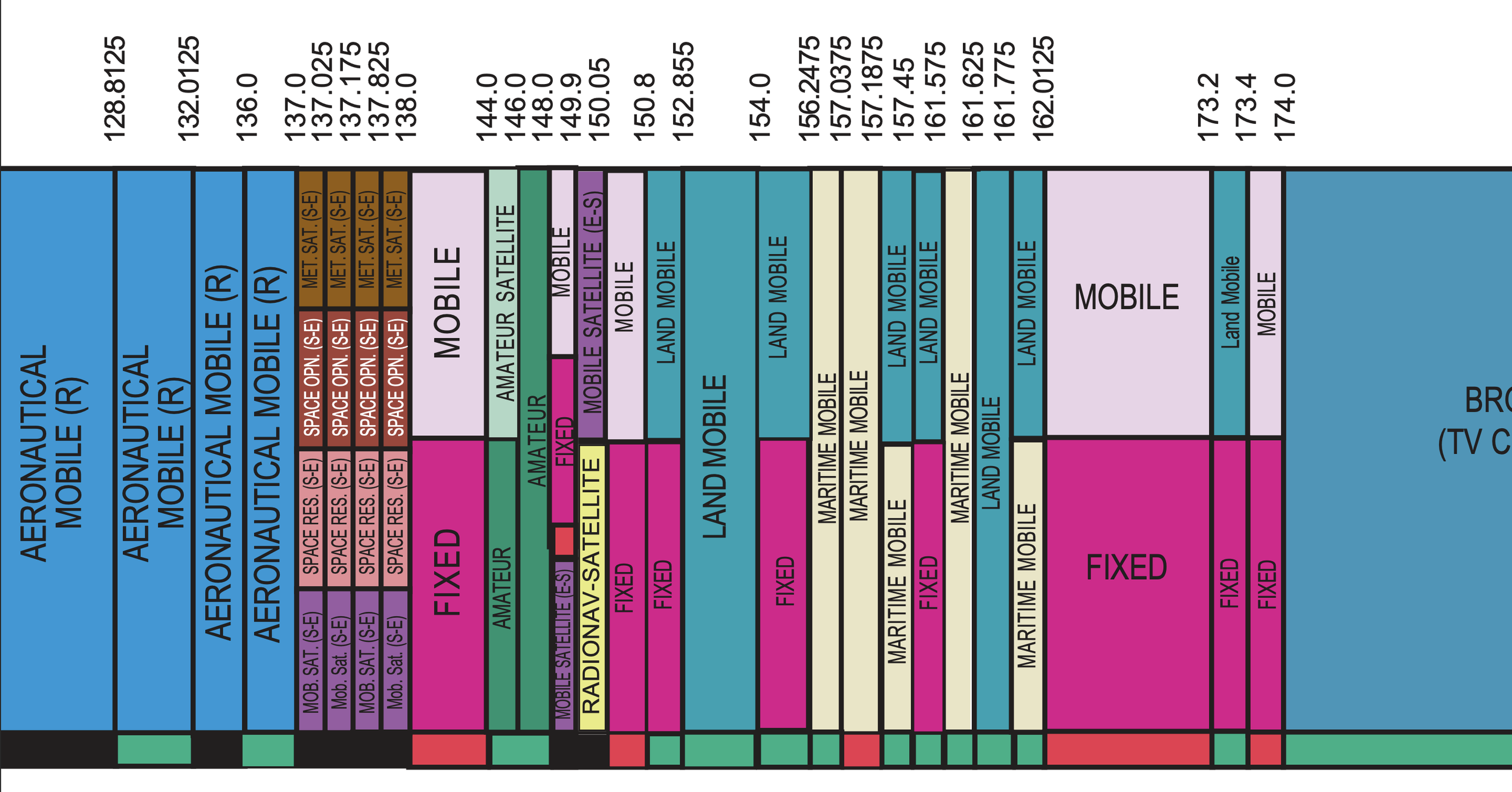
Spectrum allocation - our satellite is in brown, from 137.0 to 138.0 MHz
Land mobile radio & amateur radio is very close as well, so we want the bandwidth to be pretty small. We also want the insertion loss to be less than ~1 db at our operating frequency, ideally - although this might not be as important with an amplifier immediately following the signal.
Next, we have to choose the roll-off rate. For a small bandwidth, and a tight frequency allocation in the area of our signal, a steeper roll-off will serve well. We also need to decide on a stop-band attenuation; usually, -60 db is a good benchmark. Linear phase response within the bandwidth of our signal is also a must in order not to distort our signal.
In order for a filter to achieve these greedy margins, we need to tolerate some amount of ripple in the passband in order to achieve what we want. So, I decided to try and model everything with a 3rd order elliptical filter. I modeled it in ltspice, and found this nice looking frequency & phase response.
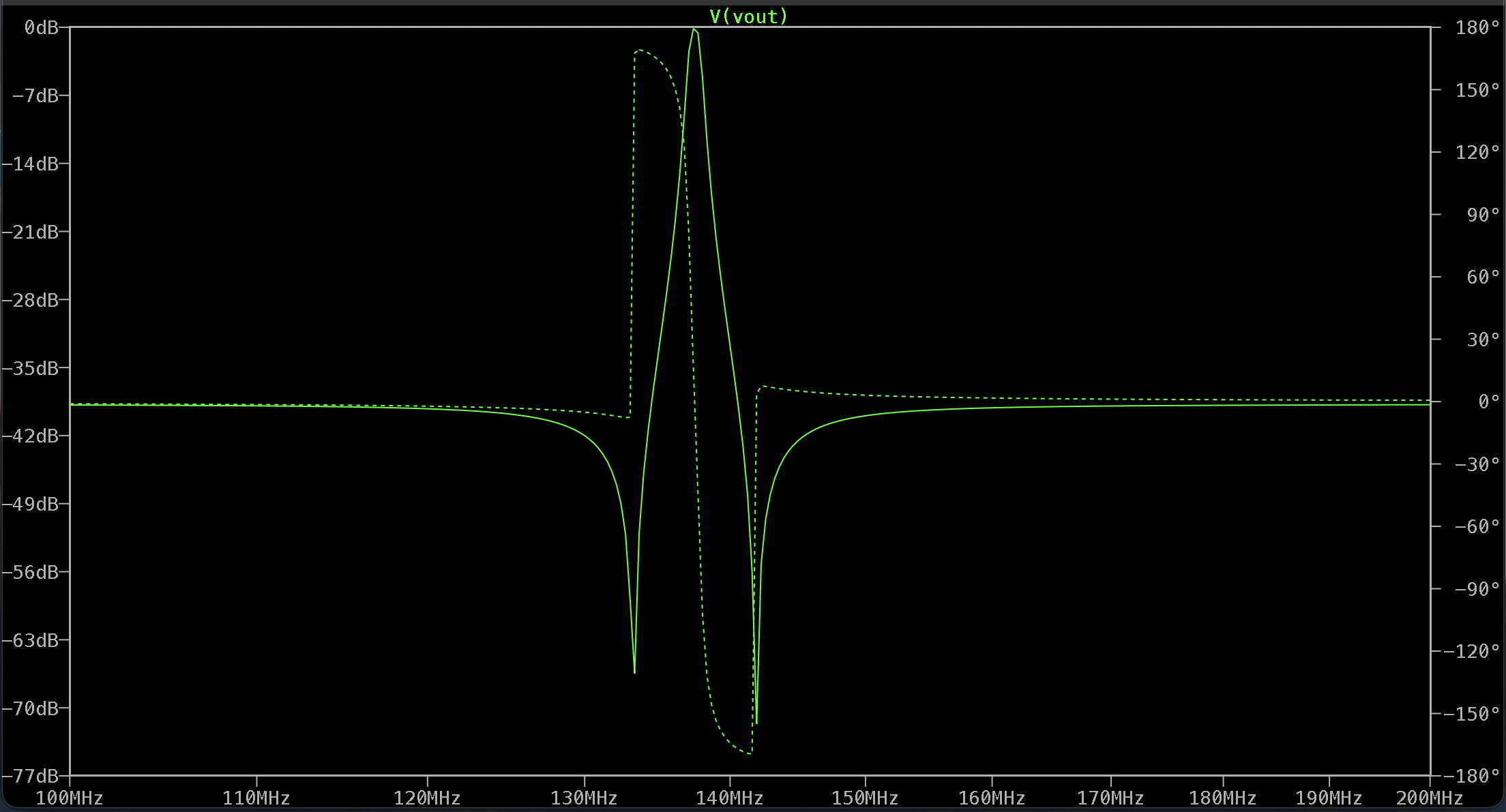
Now the hard part is to actually build it - as an ideal model with infinite Q components, this works great. But real capacitors and inductors are not ideal. All sorts of parasitics shift the response, so I’ll need to find parts for the circuit, model their parasitics, and adjust from there.
Building the PCB for this will also require some careful thinking. Improper grounding, lack of return paths, placement, trace length, and parasitic inductance & capacitance will all play a role in changing the fragile response of discrete components at higher frequencies.
Keep an eye out for more updates!